


 The Right Approach: I Hear the Train A Comin'
 It’s Only Common Sense: OCCAM—the Time Is Now
 Marcy's Musings: The Growing Industry
Research Achievement Paves the Way to GaN Power Technology at High Voltages above 650V
April 11, 2018 | ImecEstimated reading time: 3 minutes
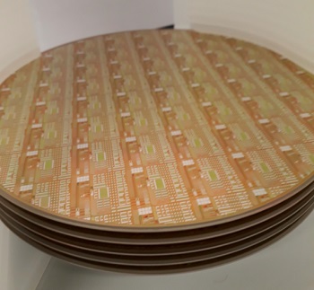
World-leading research and innovation hub in nanoelectronics and digital technologies imec, and fabless technology innovator Qromis, have announced the development of high performance enhancement mode p-GaN power devices on 200mm engineered Coefficient of Thermal Expansion (CTE)-matched substrates, processed in imec’s silicon pilot line. The substrates are offered by Qromis as commercial 200mm QST substrates as part of their patented product portfolio. The results will be presented at next week’s CS international Conference (April 10-11, Brussels, Belgium).
Today, GaN-on-Si technology is the industry standard platform for commercial GaN power switching devices for wafer diameters up to 150mm/6 inch. Imec has pioneered the development of GaN-on-Si power technology for 200mm/8 inch wafers and qualified enhancement mode HEMT and Schottky diode power devices for 100V, 200V and 650V operating voltage ranges, paving the way to high volume manufacturing applications. However, for applications beyond 650V such as electric cars and renewable energy, it has become difficult to further increase the buffer thickness on 200mm wafers to the levels required for higher breakdown and low leakage levels, because of the mismatch in coefficient of thermal expansion (CTE) between the GaN/AlGaN epitaxial layers and the silicon substrate. One can envisage to use thicker Si substrates to keep wafer warp and bow under control for 900V and 1200V applications, but practice has learned that for these higher voltage ranges, the mechanical strength is a concern in high volume manufacturing, and the ever thicker wafers can cause compatibility issues in wafer handling in some processing tools.
Carefully engineered and CMOS fab-friendly QST® substrates with a CTE-matched core having a thermal expansion that very closely matches the thermal expansion of the GaN/AlGaN epitaxial layers, are paving the way to 900V-1200V buffers and beyond, on a standard semi-spec thickness 200mm substrate. Moreover, QST® substrates open perspectives for very thick GaN buffers, including realization of free-standing and very low dislocation density GaN substrates by >100 micron thick fast-growth epitaxial layers. These unique features will enable long awaited commercial vertical GaN power switches and rectifiers suitable for high voltage and high current applications presently dominated by Si IGBTs and SiC power FETs and diodes.
“QST® is revolutionizing GaN technologies and businesses for 200mm and 300mm platforms”, stated Cem Basceri, President and CEO of Qromis. “I am very pleased to see the successful demonstration of high performance GaN power devices by stacking leading edge technologies from Qromis, imec and AIXTRON,” Basceri said.
In this specific collaboration, imec and Qromis developed enhancement mode p-GaN power device specific GaN epitaxial layers on 200mm QST® substrates, with buffers grown in AIXTRON’s G5+ C 200mm high volume manufacturing MOCVD system.
Imec then ported its p-GaN enhancement mode power device technology to the 200mm GaN-on- QST substrates in their silicon pilotline and demonstrated high performance power devices with threshold voltage of 2.8 Volt.
“The engineered QST® substrates from Qromis facilitated a seamless porting of our process of reference from thick GaN-on-Si substrates to standard thickness GaN-on- QST® substrates using the AIX G5+ C system, in a joint effort of imec, Qromis and AIXTRON,” stated Stefaan Decoutere, program director for GaN power technology at imec. The careful selection of the material for the core of the substrates, and the development of the light-blocking wrapping layers resulted in fab-compatible standard thickness substrates and first-time-right processing of the power devices.
Imec acknowledges funding from the Electronic Component Systems for European Leadership Joint Undertaking under grant agreement No 662133, designated as PowerBase.
About imec
Imec is the world-leading research and innovation hub in nanoelectronics and digital technologies. The combination of our widely acclaimed leadership in microchip technology, profound software and ICT expertise is what makes us unique. By leveraging our world-class infrastructure and local and global ecosystem of partners across a multitude of industries, we create groundbreaking innovation in application domains such as healthcare, smart cities and mobility, logistics and manufacturing, energy, and education.
As a trusted partner for companies, start-ups and universities, we bring together close to 3,500 brilliant minds from over 70 nationalities. Imec is headquartered in Leuven, Belgium, and has distributed R&D groups at a number of Flemish universities, in the Netherlands, Taiwan, USA, China, and offices in India and Japan. In 2016, imec’s revenue (P&L) totaled 496 million euro.
Further information about imec can be found here.
Share on:


Suggested Items
Real Time with… IPC APEX EXPO 2024: Tools, Training, and Trends in Manufacturing Engineering
04/25/2024 | Real Time with...IPC APEX EXPOGuest Editor Kelly Dack and Product Specialist Erik Bateham of Polar Instruments discuss Polar's latest technology, including their role in aiding manufacturing engineers. They highlight the advanced capabilities of Polar's tools and the critical role of signal integrity analysis, as well as the importance of accurate modeling in board manufacturing. Polar's unique training approach and demonstration contact details are also explored.
TTM Celebrates the Grand Opening of Its First Manufacturing Facility in Penang
04/25/2024 | TTM Technologies, Inc.TTM Technologies, Inc., a leading global manufacturer of technology solutions including mission systems, radio frequency (RF) components and RF microwave/microelectronic assemblies, and quick-turn and technologically advanced printed circuit boards (PCBs), officially opened its first manufacturing plant in Penang, Malaysia with an investment of USD200 million (approximately RM958 million).
Listen Up! The Intricacies of PCB Drilling Detailed in New Podcast Episode
04/25/2024 | I-Connect007In episode 5 of the podcast series, On the Line With: Designing for Reality, Nolan Johnson and Matt Stevenson continue down the manufacturing process, this time focusing on the post-lamination drilling process for PCBs. Matt and Nolan delve into the intricacies of the PCB drilling process, highlighting the importance of hole quality, drill parameters, and design optimization to ensure smooth manufacturing. The conversation covers topics such as drill bit sizes, aspect ratios, vias, challenges in drilling, and ways to enhance efficiency in the drilling department.
Elevating PCB Design Engineering With IPC Programs
04/24/2024 | Cory Blaylock, IPCIn a monumental stride for the electronics manufacturing industry, IPC has successfully championed the recognition of the PCB Design Engineer as an official occupation by the U.S. Department of Labor (DOL). This pivotal achievement not only underscores the critical role of PCB design engineers within the technology landscape, but also marks the beginning of a transformative journey toward nurturing a robust, skilled workforce ready to propel our industry into the future.
Fujitsu, METRON Collaborate to Drive ESG Success
04/24/2024 | JCN NewswireFujitsu Limited and METRON SAS, a French cleantech company specializing in energy management solutions for industrial decarbonization, today announced a strategic initiative to contribute to the realization of carbon neutrality in the manufacturing industry.