


 It’s Only Common Sense: OCCAM—the Time Is Now
 Marcy's Musings: The Growing Industry
 Dan’s Biz Bookshelf: Seeing the How
Golden Path Towards New Two-Dimensional Semiconductors
April 11, 2019 | Michigan Technological UniversityEstimated reading time: 3 minutes
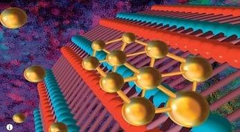
Two-dimensional (2D) semiconductors are promising for quantum computing and future electronics. Now, researchers can convert metallic gold into a semiconductor and customize the material atom-by-atom on boron nitride nanotubes.
Gold is a conductive material already widely used as interconnects in electronic devices. As electronics have gotten smaller and more powerful, the semiconducting materials involved have also shrunk. However, computers have gotten about as small as they can with existing designs — to break the barrier, researchers dive into the physics underlying quantum computing and the unusual behaviors of gold in quantum mechanics.
Researchers can convert gold into semiconducting quantum dots made of a single layer of atoms. Their energy gap, or bandgap, is formed by the quantum confinement — a quantum effect when materials behave like atoms as their sizes get so small approaching the molecular scale. These 2D gold quantum dots can be used for electronics with a bandgap that is tunable atom-by-atom.
Making the dots with monolayer of atoms is tricky and the bigger challenge is customizing their properties. When laid out on boron nitride nanotubes, researchers from Michigan Technological University have found that they can get gold quantum dots to do the near-impossible. The mechanisms behind getting gold dots to clump atom-by-atom is the focus of their new paper, recently published in ACS Nano
Energy Selective Deposition
Yoke Khin Yap, professor of physics at Michigan Tech, led the study. He explains that the behavior his team observed — atomic-level manipulation of gold quantum dots — can be seen with a scanning transmission electron microscope (STEM). The STEM’s high-powered beam of electrons enables researchers like Yap to watch atomic movement in real-time and the view reveals how gold atoms interact with the surface of boron nitride nanotubes. Basically, the gold atoms glide along the surface of the nanotubes and, they stabilize in a hover just above the hexagon honeycomb of the boron nitride nanotubes.
The atomic skiing and stopping is related to the so-called energy selective deposition. In the lab, the team takes an array of boron nitride nanotubes and runs a gold-laden mist past it; the gold atoms in the mist either stick as multilayered nanoparticles or bounce off the nanotube, but some of the more energetic ones glide along the circumference of the nanotube and stabilize, then start to clump into monolayers of gold quantum dots. The team shows that gold preferentially deposits behind other gold particles that have stabilized.
“The surface of boron nitride nanotubes are atomically smooth, there are no defects on the surface, it’s a neatly arranged honeycomb,” Yap said, adding that the nanotubes are chemically inert and there is no physical bond between the nanotubes and gold atoms. “It’s much like skiing: You can’t ski on a bumpy and sticky hill with no snow, ideal conditions make it much better. The smooth surface of the nanotubes is like fresh powder.”
Dream Nanotechnology
The search for new materials for future electronics and quantum computing has led researchers down many paths. Yap hopes that by demonstrating the effectiveness of gold, other researchers will be inspired to pay attention to other metal monolayers at the molecular-scale.
“This is a dream nanotechnology,” Yap said. “It is a molecular-scale technology tunable by atom with an ideal bandgap in the visible light spectra. There is a lot of promise in electronic and optical devices.”
The team’s next steps include further characterization and incorporating device fabrication to demonstrate all-metal electronics. Potentially, monolayers of metal atoms could make up the entirety of future electronics, which will save a lot of manufacturing energy and materials.
This work was performed in collaboration Ravindra Pandey, professor of physics at Michigan tech, whose team contributed the theoretical model, and Juan-Carlos Idrobo, scientist at the Center for Nanophase Materials Sciences at Oak Ridge National Laboratory.
About Michigan Technological University
Michigan Technological University is a public research university, home to more than 7,000 students from 54 countries. Founded in 1885, the University offers more than 120 undergraduate and graduate degree programs in science and technology, engineering, forestry, business and economics, health professions, humanities, mathematics, and social sciences. Our campus in Michigan’s Upper Peninsula overlooks the Keweenaw Waterway and is just a few miles from Lake Superior.
Share on:


Suggested Items
Boeing's Janene Stinson Earns IPC Excellence in Education Award at IPC APEX EXPO 2024
04/22/2024 | IPCThe IPC Excellence in Education award was presented to Janene Stinson, Boeing, at IPC APEX EXPO 2024 in Anaheim, California, in recognition of her significant contributions to workforce development and leadership.
Zentech’s Board of Directors Announces the Return of Matt Turpin as President and CEO
04/22/2024 | Zentech ManufacturingTurpin draws upon over 35 years of experience in the electronics industry and has an 18-year history with Zentech. He previously served as President and CEO from 2006 to 2019 after which time he has remained active in the EMS industry as an advisor to Zentech and other industry organizations.
IDTechEx Report Unveils 3D Electronics Status and Opportunities
04/22/2024 | PRNewswire3D electronics is an emerging manufacturing approach that enables electronics to be integrated within or onto the surface of objects. 3D electronic manufacturing techniques empower new features, including mass customizability, greater integration, and improved sustainability in the electronics industry.
IDTechEx Examines the Opportunities for Wearables in Digital Health
04/19/2024 | IDTechExIDTechEx’s report, “Digital Health and Artificial Intelligence 2024-2034: Trends, Opportunities, and Outlook”, covers this ongoing trend in the consumer health wearables market and includes analysis of the opportunities and roadmap for biometric monitoring.
ZESTRON Welcomes Whitlock Associates as New Addition to their Existing Rep Team in Florida
04/19/2024 | ZESTRONZESTRON, the leading global provider of high-precision cleaning products, services, and training solutions in the electronics manufacturing and semiconductor industries, is thrilled to announce the addition of Whitlock Associates to its esteemed network of sales representatives.